NVIDIA Ampere uses TSMC’s 7nm; Samsung begins work on 5nm chipset production, says report
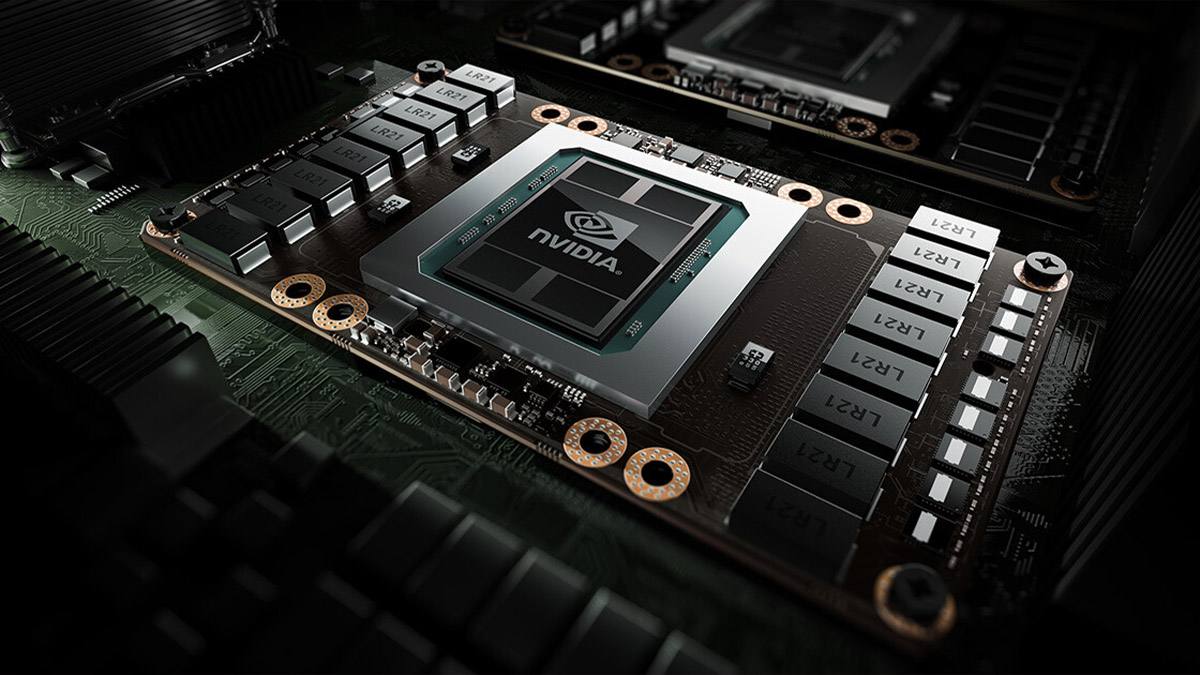
ChinaTimes in its report said, NVIDIA’s Ampere GPUs (Graphics Processing Units) are going to use Taiwan Semiconductor Manufacturing Company’s (TSMC) 7nm process node technology.
However, the next-gen Hopper Graphics Processing Unit (GPU) family would be based on the Samsung 5nm EUV process technology.
Samsung reportedly to start manufacturing 5nm chipsets:
According to the website, Samsung is planning to kickstart production of 5nm chipsets at its plant in Hwaseong, South Korea. The plant is equipped with state-of-the-art technology, besides having the capability to produce chipsets as small as 3nm.
It is worth noting that the world’s second-largest chipset maker has already begun production of 6nm and 7nm Extreme Ultraviolet chipsets.
NVIDIA’s GTC 2020:
• NVIDIA has announced to hold the much-awaited annual Graphics Technology Conference 2020 on 14th May, 2020 on its YouTube channel at 6 am PT.
• The keynote will be led by Jensen Huang, Nvidia CEO, who will highlight the firm’s latest innovations in data science, healthcare, graphics, autonomous machines, Artificial Intelligence and high-performance computing.
• The keynote was originally scheduled for March 23. Later, it was postponed due to the outbreak of COVID-19.
• The core segment of the pre-recorded keynote will focus on the Ampere GPU which is likely to be unveiled.